The United States is in the middle of the largest industrial construction campaign in a generation. Driven by the CHIPS and Science Act, national security imperatives, and the insatiable demand for AI compute, semiconductor fabrication plants are rising across the country at a pace and scale that has no modern precedent. As someone who works with contractors and manufacturers on their risk programs, the scope of what is being built right now is worth understanding -- because it is reshaping the construction industry itself.
The Scale of the Buildout
Globally, semiconductor companies plan to invest roughly $1 trillion through 2030 in new fabrication plants, according to McKinsey. A disproportionate share of that capital is flowing into the United States, fueled by $52.7 billion in federal subsidies under the CHIPS Act -- $39 billion of which is earmarked specifically for fab construction.
The projects are staggering in their individual scale. TSMC is investing $65 billion across what could eventually be six fabs and an advanced packaging facility in Arizona. The first fab entered high-volume production in late 2024, construction on the second is complete with tool installation planned for 2026, and ground has already been broken on the third. Samsung is building a semiconductor campus in Taylor, Texas, that spans 1,268 acres -- large enough for up to ten advanced fabs -- with total investment now reaching $37 billion. Intel's Ohio One project is a $28 billion complex in New Albany designed for the company's next-generation 14A process node, with underground construction complete on both fab modules and above-ground work accelerating. Micron has a $30 billion expansion underway in Boise, Idaho, and plans for a multi-phase megafab in New York that could total $100 billion over the coming decade.
These are not just large construction projects. They are among the most complex and technically demanding buildings ever constructed on U.S. soil.
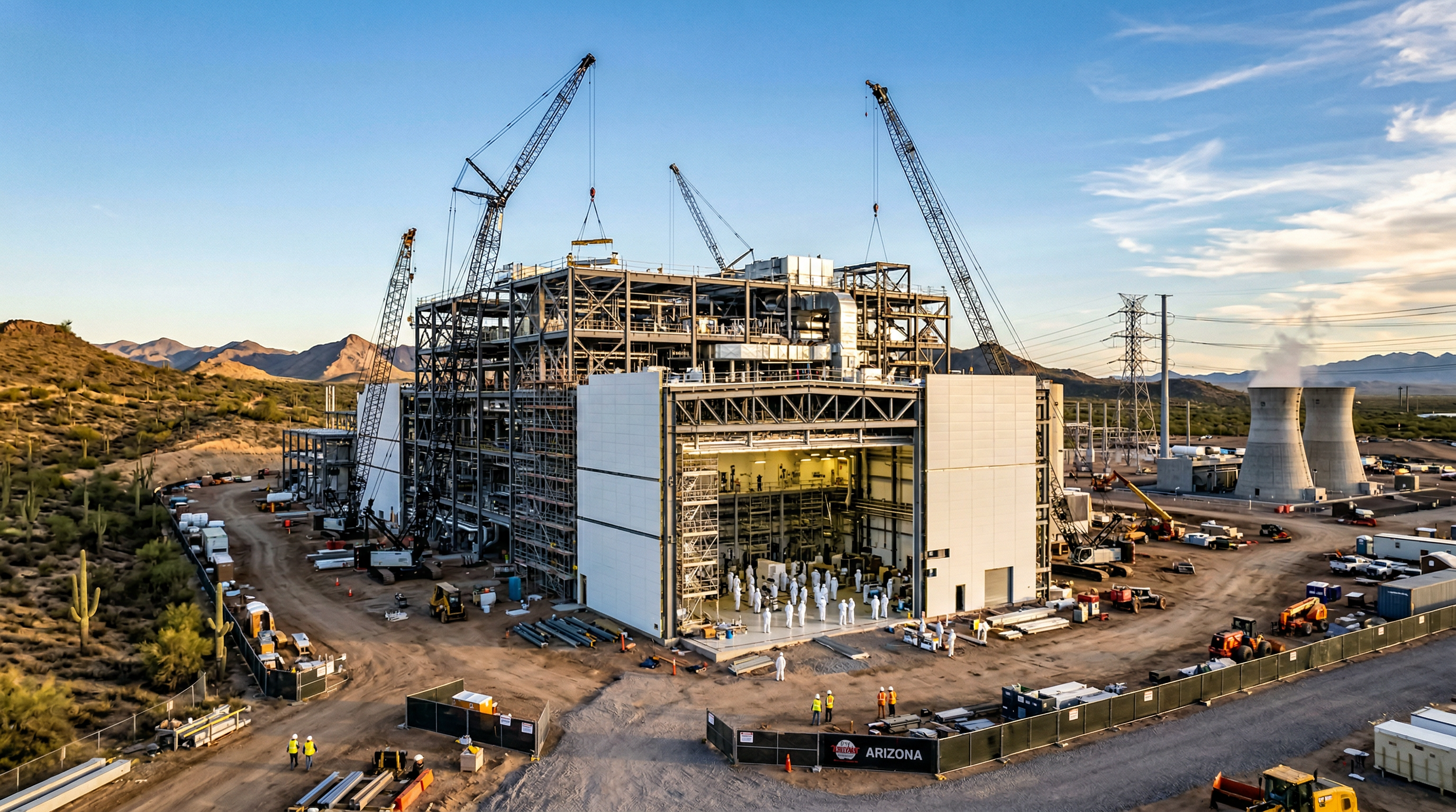
Why This Is Different from Other Construction
A semiconductor fab is not a warehouse with expensive equipment inside. These are precision-engineered environments where vibration tolerances are measured in nanometers and air purity exceeds that of an operating room by orders of magnitude. The clean room floors alone require foundations engineered to isolate even the faintest ground vibration from nearby highway traffic or rail lines. The mechanical and electrical systems that maintain temperature, humidity, and particle counts are extraordinarily complex, and the equipment being installed -- EUV lithography machines from ASML that cost $350 million each -- demands infrastructure that most construction teams have never encountered.
Building a semiconductor fab in the United States takes over 50 months from groundbreaking to volume production -- nearly double the 28-32 month timeline that is standard in East Asia. Labor costs, permitting, and a workforce that has not built fabs at this scale in decades are the primary drivers.
McKinsey's analysis underscores the cost challenge: even with CHIPS Act subsidies accounted for, a standard mature logic fab built in the United States costs roughly 10 percent more to construct and carries up to 35 percent higher operating costs than a comparable facility in Taiwan. U.S. construction labor costs for fab-specific trades run four to five times higher on an hourly basis than in Asia. And because significant fab construction has not occurred in the U.S. at this scale in decades, the available workforce has less experience, which reduces productivity and extends timelines further.
The workforce challenge is acute. The semiconductor industry needs an estimated 170,000 or more new workers in the U.S. over the next five years, spanning everything from clean-room technicians to the specialized construction trades -- electrical, controls, instrumentation, welding -- required to build these facilities. Contractors with national labor access and prefabrication capabilities have a meaningful competitive advantage.
Where the Major Projects Stand
TSMC's Arizona operation is the furthest along and the current benchmark for U.S. fab construction execution. The first fab is producing 10,000 to 30,000 wafers per month using the 4-nanometer process. The second fab, targeting 3-nanometer production, is now expected to begin high-volume manufacturing in the second half of 2027 -- pulled forward a year from the original schedule due to strong customer demand. Permits are being sought for a fourth fab and the company has purchased additional land to support what it describes as "very strong AI-related demand."
Samsung's Taylor campus has seen a more complicated trajectory. After delays from foundry market uncertainty and subsidy timing, the company received $4.75 billion in CHIPS Act funding and secured a major anchor customer in Tesla, which signed a $16.5 billion agreement for AI chip production. Samsung's first Taylor fab is on track to begin mass production in 2027, and a second fab has entered preliminary regulatory review. The site is designed to target 50,000 wafer starts per month -- exceeding the capacity of both Intel's Fab 52 in Arizona and TSMC's typical individual fab modules.
Intel's Ohio project has faced the most visible delays, with the original 2025 production target pushed to 2030 for the first module and 2031 for the second. But activity has accelerated: total Ohio investment has surpassed $5 billion, all major underground construction is complete, above-ground structural work is progressing, and the company has partnered with nearly 450 Ohio suppliers. The $8.9 billion in remaining CHIPS Act funding released to Intel has given the project renewed momentum.
Micron's Boise expansion expects first wafer output in the second half of 2027, while its New York megafab timeline has been pushed from 2028 to 2030 for the initial phase, with subsequent phases extending through 2041.
The Bottom Line
What is happening in semiconductor construction right now is not just a cyclical uptick -- it is a structural transformation of American industrial capacity. The combination of federal investment, AI-driven demand, and geopolitical urgency has created a construction pipeline that will take the better part of a decade to execute. For the construction industry, these projects represent some of the most demanding and highest-value work available anywhere in the country. For manufacturers, they signal a fundamental reshoring of the most strategically important supply chain in the global economy.
The challenges are real -- cost premiums, workforce shortages, extended timelines, and technical complexity that dwarfs conventional construction. But the capital is committed, the ground is broken, and the fabs are going up. This is the industrial bet of our generation, and its outcome will shape American manufacturing competitiveness for decades to come.
Working on Industrial or Manufacturing Construction?
I work with contractors and manufacturers on risk programs designed for technically complex, high-value projects. If you are involved in semiconductor or advanced manufacturing construction, I would welcome the chance to discuss your risk strategy.
Get in Touch